-
Courses

Courses
Choosing a course is one of the most important decisions you'll ever make! View our courses and see what our students and lecturers have to say about the courses you are interested in at the links below.
-
University Life

University Life
Each year more than 4,000 choose University of Galway as their University of choice. Find out what life at University of Galway is all about here.
-
About University of Galway

About University of Galway
Since 1845, University of Galway has been sharing the highest quality teaching and research with Ireland and the world. Find out what makes our University so special – from our distinguished history to the latest news and campus developments.
-
Colleges & Schools
Colleges & Schools
University of Galway has earned international recognition as a research-led university with a commitment to top quality teaching across a range of key areas of expertise.
-
Research & Innovation
Research & Innovation
University of Galway’s vibrant research community take on some of the most pressing challenges of our times.
-
Business & Industry
Guiding Breakthrough Research at University of Galway
We explore and facilitate commercial opportunities for the research community at University of Galway, as well as facilitating industry partnership.
-
Alumni & Friends

Alumni & Friends
There are 128,000 University of Galway alumni worldwide. Stay connected to your alumni community! Join our social networks and update your details online.
-
Community Engagement
Community Engagement
At University of Galway, we believe that the best learning takes place when you apply what you learn in a real world context. That's why many of our courses include work placements or community projects.


MEF
Metal Enhanced Fluorescence:
 The Metal Enhanced Fluorescence (MEF) effect is the observed increase in the quantum yield, and reduction in fluorescence lifetime, of weakly emitting fluorophores that are held in close proximity to noble metal surfaces that are roughened on the nanometre scale.
The first part of the project involves fabricating different nanopatterned surfaces using both advanced laser processing methods and chemical deposition routes. The next part of the project involves studying the fundamental physics and chemistry of the MEF effect on these surfaces. This end goal is to develop ultra-sensitive measurement methods down to single molecule level suitable for use in microarrays and sensing applications.
Introduction: One route to increased sensitivity for assays and microarrays is to utilise the Metal Enhanced Fluorescence (MEF) effect. This is the dramatic increase in the fluorescence emission of fluorophores held at precise distances (50 to 200 Å) above nanoroughened metal surfaces [i, ii, iii, iv, v, vi]. The MEF effect derives from the interaction of the dipole moment of the fluorophore and the surface plasmon field of the metal resulting in an increase in the radiative decay rate and stronger fluorescence emission. In effect, this means that weakly emitting materials (dyes, proteins, or DNA [vii]) with low quantum yields can be transformed into more efficient fluorophores and shorten the fluorescence lifetime as well. The reduction in fluorescence lifetime due to MEF means that molecules spend less time in the excited state, thus reducing photobleaching effects [iii]. This enables the use of photosensitive fluorophores that may not have been considered previously because of high photobleaching rates. Another interesting effect occurs when fluorescence originates from above periodic nanopatterned materials. In this case, the fluorescence emission can be spatially directed over a small viewing angle [viii], which offers possibility of very high efficiency fluorescence emitters that can be coupled directly into detectors without extensive optics. This high directional emission combined with the increases in quantum yield offers the potential for very efficient MEF based sensors and microarrays[iii]. These unique characteristics of the MEF effect, will lead to the development of many novel fluorescence measurement methods and techniques [iii, iv].
The science of manipulating MEF is also described as Radiative Decay Engineering (RDE) since it involves controlling the radiative decay rate of fluorophores by the careful engineering of the chemical environment and physical morphology of the nanopatterned metal surfaces. To date most MEF studies have utilised Silver Island Films (SIF), which are formed either by chemical deposition from solution or by evaporation of silver under high vacuum onto quartz or glass substrates [iii]. Another critical MEF parameter is the precise distance (50-200 Å) at which the fluorophore is maintained from the metal surface. In some cases, a dielectric coating (e.g. SiO 2) of the correct thickness can be evaporated over the SIF [ix], or a molecular spacer that binds directly to metal surfaces (e.g. thiols with silver/gold) of the desired length can be used. The study of MEF and its applications is still in its infancy and there is a need to develop further our understanding of the fundamental physics and chemical processes that govern MEF before practical applications can be developed. Furthermore, there is a need for facile and reliable fabrication methods to nanopattern, with high aspect (height divided by width) ratios, a range of materials such as silicon, quartz, and silver. These methods should also be easily scaled up for the fabrication of MEF based microarrays (10 4 – 10 6 elements) suitable for the next generation of fluorescence-based microarrays [x, xi].
References:
[i] J. Kummerlen, A. Leitner, H. Brunner, F.R. Aussenegg, and A.Wokaun. "Enhanced dye fluorescence over silver island films - analysis of the distance dependence," Mol. Phys., (1993) 80(5), 1031-1046.
[ii] K. Sokolov, G. Chumanov, and T.M. Cotton. "Enhancement of molecular fluorescence near the surface of colloidal metal films," Anal. Chem. (1998) 70(18), 3898-3905.
[iii] J.R. Lakowicz. "Radiative Decay Engineering: Biophysical and Biomedical Applications," Anal. Biochem. (2001) 298, 1-24.
[iv] J.R. Lakowicz, Y. Shen, S. D’Auria, J. Malicka, J. Fang, Z. Gryczynski, and I. Gryczynski. "Radiative Decay Engineering: 2. Effects of Silver Island Films on Fluorescence Intensity, Lifetimes, and Resonance Energy Transfer," Anal. Biochem. (2002) 301, 261-277.
[v] J. DeSaja-Gonzalez, R. Aroca, Y. Nagao, and J.A. DeSaja. "Surface Enhanced Fluorescence and Raman spectra of N-Octadecyl-3,4:9,10-Perylenetetracarboxilic Monoanhydride on Silver Islands," Spectrochim. Acta (A), (1997) 53, 173-181.
[vi] T. Schalkhammer, F. R. Aussenegg, A. Leitner, H. Brunner, G. Hawa, C. Lobmaier and F. Pittner. "Detection of fluorophore-labelled antibodies by surface-enhanced fluorescence on metal nanoislands," Proc SPIE – Int. Soc. Opt. Eng., (1997) 2976, 129.
[vii] J.R. Lakowicz, B. Shen, Z. Gryczynski, S. D'Auria, and I. Gryczynski " Intrinsic Fluorescence from DNA Can Be Enhanced by Metallic Particles," Biochem. Biophys. Res. Comm., (2001) 286(5), 875-879.
[viii] S.C. Kitson, W.L. Barnes and J.R. Sambles. "Photoluminescence from dye molecules on silver gratings," Optics Communications, (1996) 122, 147-154.
[ix] P.J. Tarcha, J. DeSaja-Gonzalez, S. Rodriguez-Llorente, and R. Aroca. "Surface-Enhanced Fluorescence on SiO 2 Coated Silver Island Films," Appl. Spectrosc., (1999) 53, 43-48.
[x] C. Mayer, N. Stich, T. Schalkhammer, and G. Bauer. "Slide format proteomic biochips based on surface-enhanced nanocluster-resonance. scanners," Fres . J Anal Chem., (2001) 371, 238-245.
[xi] N. Stich, A. Gandhum, V. Matushin, C. Mayer, G. Bauer, and T. Schalkhammer. "Nanofilms and nanoclusters: Energy sources driving fluorophores of biochip bound labels," J. Nanosci. Nanotech., (2001) 1(4), 397-405.
 |
 |
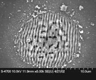 |
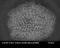
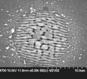
| A | B | C |
Fig. 1: (A) Scanning Electron Microscope (SEM) image showing the nanopatterned silicon processed at just below the ablation threshold using femtosecond laser pulses, (B & C) SEM images of the ripple formation on a sample rotated at right angles, these ripples remain
Our first laser processing experiments were done in February 2004 at Walter Perrie's laboratory at Liverpool University . The UV femtosecond laser facility allows the formation of much smaller ripples than those seen with 775 nm femtosecond laser processing.
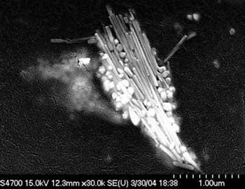 |
The image on the left shows silver nanorods that we have made recently in the laboratory. We are in the process of developing a routine method for making these rods using very simple chemistry. |